


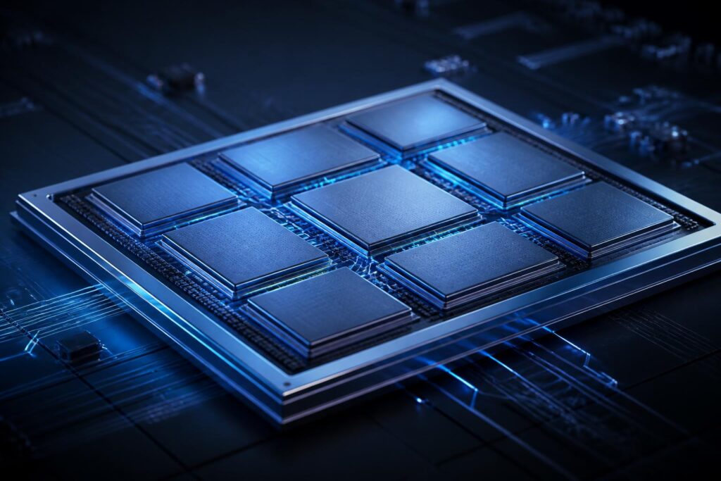
For many decades, the semiconductor industry has generally pursued a fairly clear vision of the processor: the more functions integrated onto a single piece of silicon, the more powerful and efficient the chip would be. However, as circuits have become denser, continuing to shrink every component and place them all on the same semiconductor die has become increasingly complex. Design costs have risen, testing processes have become more difficult, and even a small defective area can cause the entire chip to fail qualification.
Chiplets have emerged as an alternative approach. Instead of creating a monolithic processor, designers divide the system into multiple small modules, with each module responsible for a specific group of functions. These modules are connected within the same package so that they operate as a unified system. This is not simply a matter of connecting separate components; it represents a change in architecture, manufacturing processes, and even the way the industry plans a semiconductor product.
What Are Chiplets, and How Do They Differ from Traditional Chips?
In a monolithic design, components such as processor cores, memory controllers, accelerators, caches, and communication circuits are usually created on the same silicon die. The entire system is manufactured, tested, and packaged as one large unit. This approach has the advantage that the connections between components can be very short, while designers retain control over the entire architecture within a unified space.
With chiplets, these components can be separated into smaller dies. One chiplet may contain computing cores, another may handle communications, while another module may serve memory or a specialized task. The chiplets are then placed in the same package and linked using high-speed interconnect technology. From the user’s perspective, the system is still identified as a single processor or component, but internally it is a collection of modules that can be designed and manufactured in different ways.
The important point about this model is its separation of functions. Not every function needs to use the most advanced manufacturing process. Parts that require high circuit density can be placed on suitable chiplets, while control or communication circuits that depend less on scaling can use a different process. This gives designers more room to balance performance, cost, and energy consumption.
Why Is Modular Architecture Receiving Attention?
The first benefit is reusability. Once a chiplet has been designed and stabilized, it can become a foundation for multiple products. Manufacturers can change the number of computing modules, the cache capacity, or the type of interconnect without having to rebuild the entire chip from scratch. This approach is particularly useful for product lines with many versions, ranging from personal devices to servers and specialized computing systems.
The next benefit concerns manufacturing efficiency. A small silicon die is generally easier to control than a very large one. If a small area is defective, the impact can be limited to one chiplet instead of damaging the entire design. This does not mean that every chiplet product is automatically cheaper, since packaging, testing, and interconnection costs are also significant. Nevertheless, dividing the design creates additional options for optimizing the yield of qualified products and reducing material waste.
Chiplets also make it possible to combine different manufacturing technologies. A system can use a computing chiplet manufactured with a newer process alongside an interconnect module made using a more mature process. This flexibility means designers do not have to apply an expensive process to every part. In some cases, it can also extend the life of proven modules instead of discarding them simply because another component needs to be upgraded.
Scalability is another notable advantage. As requirements increase, a system can be built with more modules or with higher-capability chiplets. This type of expansion is not as simple as adding external components, since every chiplet must be guaranteed to meet requirements for communication, latency, power, and heat. Even so, modular architecture creates a more flexible design language than simply increasing the size of a single silicon die.
Technical Challenges That Cannot Be Overlooked
The greatest challenge for chiplets is interconnection. The modules within a system must exchange data at high speeds and with low latency. If the links are not efficient enough, the benefits of dividing the design can be negated by waiting time and the energy used to transmit data. Designers therefore have to consider protocols, physical layout, synchronization mechanisms, and signal distribution from the earliest stages.
The distance between chiplets also creates new packaging requirements. When multiple modules are concentrated in a small space, heat is no longer distributed simply. A heavily operating chiplet can affect neighboring modules. The cooling system, power supply, and packaging materials must be designed as part of the overall architecture rather than dealt with after the logic design has been completed.
Testing also becomes more complex. With a monolithic chip, manufacturers test an integrated design. With a chiplet system, they must test each module, the connections between modules, and the entire package under a range of operating conditions. A chiplet may meet requirements on its own but develop problems when working with another chiplet. Therefore, the validation process must include compatibility, link durability, and system behavior over an extended period.
There is also the issue of standards. If each manufacturer uses its own connection method, combining chiplets from multiple sources will be very difficult. A more open ecosystem could help companies choose suitable modules and shorten development time, but achieving this requires agreement on communication, testing, security, and responsibility when a product fails. This is a technical issue, but it is also a supply-chain organization challenge.
Impact on Product Design and the Market
Chiplets can change a company’s role in the semiconductor value chain. In the past, a company would often try to control most of a processor’s design. With modular architecture, a company can focus on its particular strengths, such as designing computing cores, accelerators, security circuits, or interconnect platforms. The remaining parts can come from specialized partners. This model creates opportunities for collaboration, but it also makes the management of design rights and component quality more important.
For data centers, chiplets can support the creation of processors suited to different types of workloads. A system for data analytics will have different needs from one for graphics processing, machine-learning models, or storage services. Rather than using the same design for every purpose, providers can build more modular configurations. However, the practical benefits depend on how software uses the resources and on the ability to coordinate data among the components.
In personal devices, this architecture could help create products that achieve a better balance among performance, battery life, and size. Some specialized functions could be assigned to separate modules for more efficient processing instead of forcing the main cores to handle every task. Even so, not every device needs chiplets. For products with modest requirements or insufficient production volumes, development and packaging costs may make a monolithic design the more reasonable choice.
A Foundation for Long-Term Design Thinking
The greatest value of chiplets lies not only in combining multiple pieces of silicon in the same package. More importantly, they encourage the industry to view a processor as a system that can be broken down, reused, and upgraded piece by piece. This way of thinking fits a context in which computing applications are becoming increasingly diverse while the cost of developing an entirely new product continues to rise.
It also requires a change in how performance is evaluated. It is not enough to look only at the number of cores or the processing speed of an individual chiplet. The efficiency of the entire system also depends on data-transfer capability, power consumption, latency, temperature, software, and the stability of the interconnections. A multi-module design is meaningful only when the modules work together better than a simpler alternative.
In the coming years, chiplets may continue to develop alongside new packaging and interconnection technologies. This path does not eliminate monolithic chips entirely; rather, it adds an option suited to systems that need scalability, specialization, or shorter development cycles. When deployed in the right context, modular architecture helps designers allocate resources more precisely and create products that are more flexible in response to changing needs.
The shift from one large chip to a system composed of multiple chiplets is not merely a change in physical form. It is a change in how the semiconductor industry thinks about performance, manufacturing, and upgradability. The success of chiplets will depend on solving the interconnected challenges of communication, heat, testing, standards, and software. But even if they do not become the choice for every device, this model has already opened an important path toward continuing to build more powerful computing systems without relying solely on making a single silicon die ever larger.
